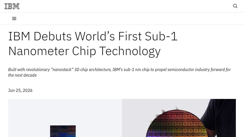
IBM debuts sub-1 nanometer chip technology(newsroom.ibm.com)
373 points by porridgeraisin | 198 comments
IBM newsroom press release announcing its first sub-1 nanometer chip technology built with a "nanostack" 3D chip architecture.
First screen, captured . Open the video.
Captured . Click for the whole screenshot.
373 points by porridgeraisin | 198 comments
IBM newsroom press release announcing its first sub-1 nanometer chip technology built with a "nanostack" 3D chip architecture.

50 points by gok | 24 comments
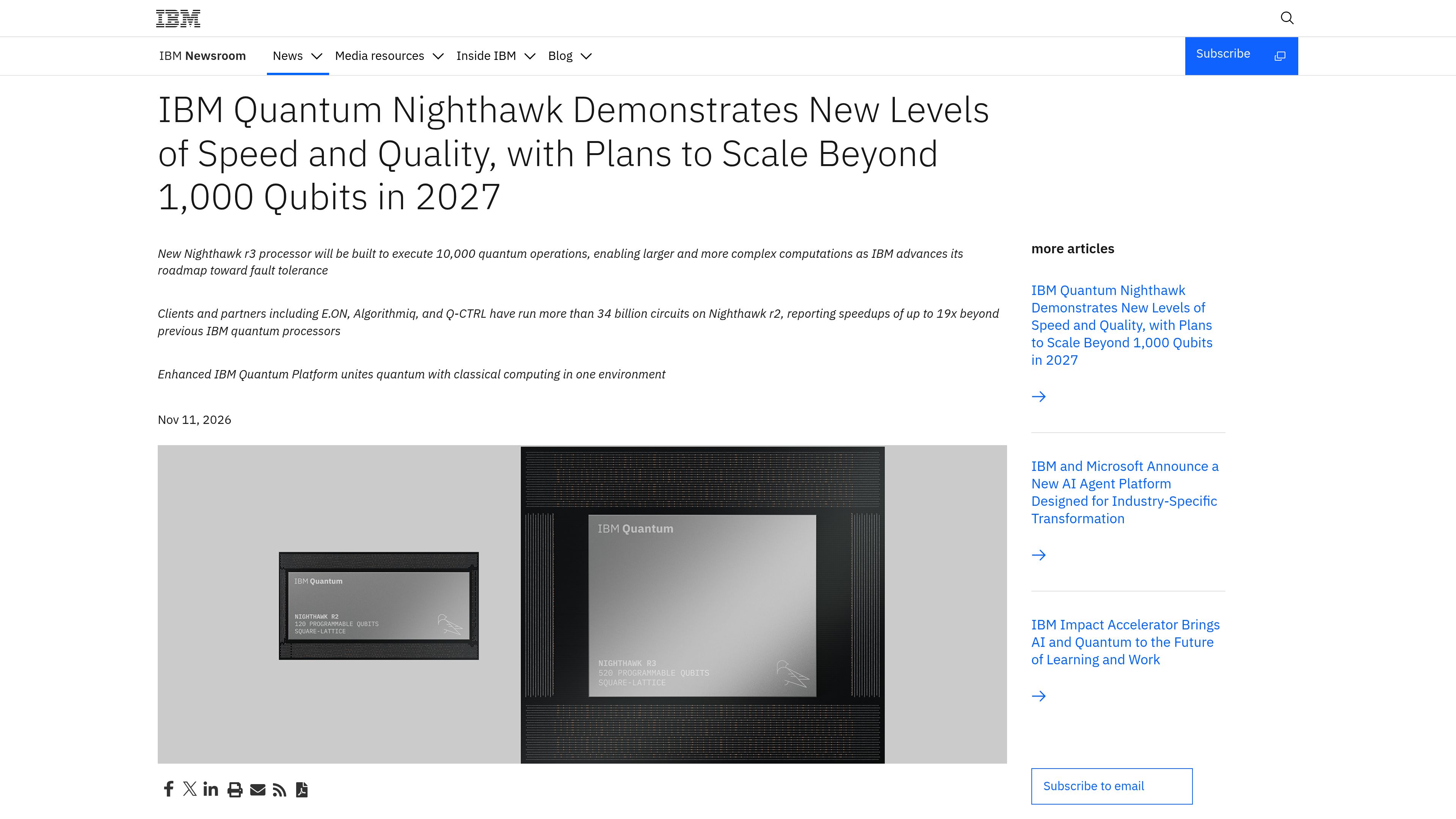
IBM press release announcing the Nighthawk r3 quantum processor (520 qubits, 10,000 operations), Nighthawk r2 results, and plans for a 1,000+ qubit system in 2027.

807 points by king_phil | 472 comments
TSMC press release announcing a joint venture with Bosch, Infineon, and NXP to build an advanced semiconductor fab in Europe, issued August 8, 2023.
402 points by rbanffy | 185 comments
NIST news release describing a method of stacking materials on silicon wafers to build photonic chips with lasers that can produce nearly any wavelength.

345 points by latchkey | 133 comments
Wafer blog post on serving the GLM-5.2 model on AMD MI355X GPUs at 2626 tok/s per node and 213 tok/s single stream, at over 2x lower cost than Nvidia Blackwell.
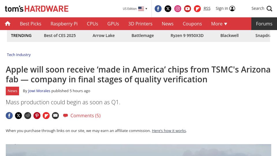
400 points by rbanffy | 365 comments
Tom's Hardware news article reporting that TSMC's Arizona fab is in final quality verification for Apple chips, with mass production possibly starting in Q1.
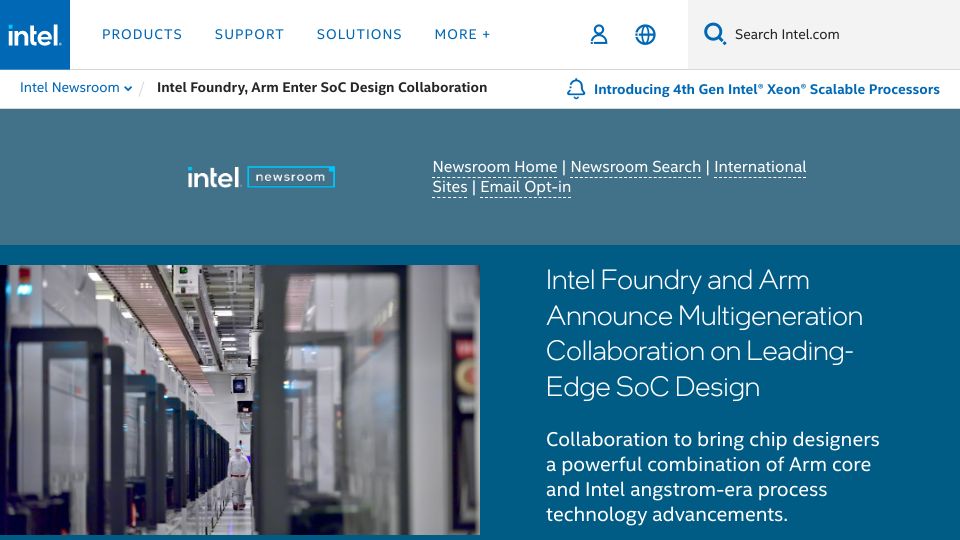
422 points by mepian | 175 comments
Intel newsroom press release announcing a multigeneration collaboration between Intel Foundry Services and Arm on leading-edge SoC design using Intel process technology.

325 points by ece20 | 578 comments
New York Times article reporting Intel will receive $8.5 billion in CHIPS Act grants to build semiconductor plants, announced by President Biden in Arizona.